
John Errington's Experiments with an Arduino
Using digital inputs: Switches and buttons
Introduction
All the Arduino family of microcontrollers have pins that may be used as inputs. This article looks at some alternative ways of connecting digital input devices - switches and buttons.
On this page:
- Pins of the arduino family
- Buttons, switches, pull up (and pull down)
- "Logic levels"
- Values for pull-up, pull down, and protection resistors
- Digital input characteristic and hysteresis levels
- Behaviour of digital pins configured as inputs
Pins of the arduino family
To give maximum flexibility each external connection on and Arduino board may share different functions. Lets look at some examples on the Arduino Nano; I'll refer to the pin numbers as shown on the board itself.
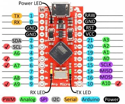
Pin 7: Digital Input or Digital Output
Pin 4: Digital Input, Digital Output or Analog input
Pin 5: Digital Input, Digital Output or Pulse Width Modulated output
Each member of the Arduino family has differences so you will need to check the pin configuration for the Arduino you are using.
However a common factor is that for all Arduinos
A pin that is not programmed behaves as a digital input,
in the same way as if it was declared as
pinMode(pin, INPUT)
In the following information, unless otherwise stated all data and values are taken from the data sheet for the ATMega328P which powers the Arduino Nano.
Most Arduinos use the 328 or 32U4 chips; the later Due, Zero and others use more powerful processors that run from 3.3V however the electrical characteristics are similar.
Now lets look at how we can provide logic input signals to the Arduino.
Buttons, switches, pull up (and pull down)
In using a switch or push button to provide a digital input to the Arduino we basically have two options as shown here; to connect one side of the switch or button to the ground 0V rail -
or to connect it to the +Vcc rail. The usual (MUCH better) choice is to use a ground connected "normally open" button or switch. This has many advantages - but the "active" (pressed) condition of the button results in a logic "0" and inactive or released condition gives a "1".

FIG 1 Here we see good and bad implementations of a push button connected between a digital pin and the ground rail.
PB1 will generate a good logic 0 when pressed; but when its open Pin D1 will be floating and give unpredictable results. Most likely it will NOT immediately go to a logic 1 when released.
HOWEVER if you configure the input as "INPUT_PULLUP" the Arduino connects an internal pull up resistor - so it behaves like the nest circuit (PB2/D2)
The circuit around PB2 / Pin D2 shows a correct implementation; before the button is pressed, and after it is released, Rpu the external pull-up resistor will ensure it is at the correct voltage to generate a good logic 1.
Button connected to the +Vcc rail
Here we see a button connected to the Vcc rail. Pin D3 will be at a logic "1" when the PB3 button is pressed - but when its released the value will be indeterminate because the input is floating.
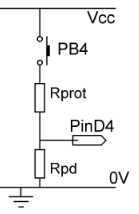
PB4 shows the "correct" implementation. We need a "pull-down" resistor Rpd to ensure Pin D4 is at a logic zero when the button is released.
Its also good practice to include a "protection" resistor, Rprot as if the button is inadvertently wired to the wrong supply rail an excessive current can flow into the pin, damaging the circuit.
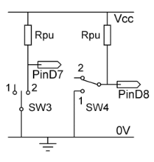
Here we see switches used to provide inputs.
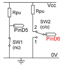
FIG 2 The first figure here shows a switch connected to the ground rail, with a pull-up resistor. It will work fine, giving a good "logic 0" voltage at pin D5, and changing to a good "logic 1" when activated. As before you can configure the pin as "INPUT_PULLUP" when an external pullup resisitor will not be required.
So what is wrong with the next circuit? We are using a change-over switch, with an external resistor.
With SW2 in position 1 a good logic zero appears at pin D6. When its in position 2 D6 gets a good logic 1.
The problem is that as the switch passes between those positions the D6 input is left open-circuit and logic level undefined.
This issue is fixed by moving the pull-up resistor as shown below SW4 / D8. As soon as the switch leaves position 1 Rpu takes the voltage to logic 1.
On this page you can see how a multi-way switch can be used and coded with diodes to reduce the number of inputs that need to be committed; for example a 12 way switch could be coded to need only 4 digital pins.
"Logic levels"
 FIG 3 This diagram shows the "logic levels" for the 328 and 32U4 processors when used on a 3.3V or 5V supply.
So for a Nano or Pro Micro running from a 5V supply we see:
- Input pin voltages above 5V or below 0V are not allowed as they would damage the processor.
- A voltage between 3.0V and 5.0V will be read as a logic "1"
- A voltage between 0.0V and 1.5V will be read as a logic "0"
- A voltage between 1.5V and 3.0V will always give a reading of a "1" or a "0" ..
- but we cant say which it will be. This region gives an "undefined" value, so in normal use we must avoid such an input voltage.
More about the "undefined" region in the section below on hysteresis.
Values for pull-up, pull down, and protection resistors
For most purposes the internal pull-up resistor is sufficient. It is connected by declaring a pin as pinMode(pin, INPUT_PULLUP) and would replace the external pull-ups shown above.
Normally you should choose to connect your switches to the ground rail.
Why? because if power is removed from the Arduino a pin that stays connected to a positive supply can allow current to flow and damage the circuit.
Also, common practise is to make a ground connection widely available as a reference, while your Vcc ONLY connects where it is needed. Thats why the Arduino offers "INPUT_PULLUP" rather than "pull down".
Depending on the particular board used the "INPUT_PULLUP" value will most likely be between 20k and 150k.
This can leave the input susceptible to noise, so if you are using an external pull-up you may wish to use a smaller value.
The switch circuit will draw current from the supply when the switch is closed. EG with a 1k pull-up a current of 5v/1k - 5mA will flow; so to keep current consumption down its usual to use pull-up values of 5k upwards.
If you MUST use a positive voltage input
 In this circuit we need to be more careful. The pin should be declared as pinMode(pin, INPUT) which disconnects the internal pull-up resistor.
Now the pull-down resistor can be any practical value, because of the high input resistance of the Arduino pin. However
a high impedance is a disavantage in digital circuit as it exposes the connection to picking up stray signals; So
Lets choose a value for Rpd of 10kOhm. When PB4 is open Pin D4 will be at or around 0V.
Now if Vcc matches Vcc for the Arduino we need to choose Rprot so that Pin D4 lies securely in the logic 1 region when the switch is closed. For all Arduinos a voltage between Vcc and 0.7*Vcc will be a good logic 1.
So, if we choose 3k3 for Rprot the voltage on D4 will be Vcc * Rpd/Rprot + Rpd = Vcc * 10k/10k + 3.3k = 0.75 * Vcc
That's a good logic 1. You can adjust the value chosen for Rprot to suit any external positive voltage.
We can debounce the switch action by adding a small capacitor from D4 to ground. (see next section)
Digital input characteristic and hysteresis levels
How the digital input circuit responds to a changing voltage at the input

This graph shows how an input voltage on a digital input will be treated.
The top (red VIH) line shows the voltage above which an input will DEFINITELY be recorded as a "HIGH"
A voltage below the (DARK BLUE VIL) line will DEFINITELY be read as a "LOW" or logic "0"
The orange "Vih" and cyan "Vil" lines show hysteresis levels. For Arduino's running from a 5V supply these voltages are
VIH = 3.0V; Vih = 2.6V; Vil = 2.2V; VIL = 1.5V
The effect of these hysteresis levels is shown on the next graph
 This shows how the digital input responds to a changing signal. The blue line shows a ramp voltage applied to a digital input pin. It starts at just over 1V which is in the "logic 0" region between 0V and VIL; so of course this is read by the arduino as a logic "0". The red line represents the logic level.
Note the logic level stays at zero as we move above VIL. We are now in the "indeterminate" band, and it is the hysteresis levels that determine how the input will be represented.
The logic level does not change until Vin exceeds Vih. At that point it transitions to a logic "1". It remains there as we pass into the "logic 1" region between VIH and Vcc.
Now as the input voltage is decreasing, the logic level remains at a "1" as Vin falls out of the "logic 1" band; and stays at a "1" until Vin < Vil.
At that point, still in the "indeterminate" band, the logic level falls to a "0"
Behaviour of digital pins configured as inputs
If you need to drive a logic input from an external circuit - something other than a button or switch - you need to know the electrical characteristics of the input circuit.

A digital pin configured as an input has a very high impedance; in effect it behaves very much like an open circuit. The CMOS circuit presents a very high resistance, and can pick up stray signals or static electricity which could damage the circuit. Diodes D1 and D2 prevent this by constraining the input to voltages between 0V and Vcc.
Input voltage: Vin >0V and Vin <Vcc
Input resistance Rin >100Mohm
The 32U4 and 328 data sheets show the maximum value of leakage current at an input pin as 1uA. This corresponds to an effective input resistance of MORE THAN 5Mohm. However the data sheet for the ATMel Cortex SAM3 as used on the Arduino Zero and Due gives a more realistic value typically of 2 - 5 nA.
5V/5nA = 1Gohm.
Input capacitance Cin - "typically a few pF"; I havent been able to find a specified value for this but this is the general guidance for many CMOS circuits.