John Errington's tutorial on Power Supply Design
Voltage regulation: Conclusion
The previous pages give a thorough and detailed description allowing the design of a regulated power supply.
I offer here some suggestions for component choice, and notes about heat sinking.
Suitable transistors
| Type no | Vceo/Vcbo | Ic | Pt | Hfe | deg C/W | Type | Package |
|---|---|---|---|---|---|---|---|
| BC546B | 65V | 100mA | 0.6W | 150 | 83 | NS | TO92 |
| BD139 | 80V | 1.5A | 12.5W | 250 | 10 | NS | TO126 |
| TIP120 | 60V | 5A | 65W | 1000 | 2.0 | ND | TO220 |
| BDX33C | 100V | 10A | 70W | 750 | 1.8 | ND | TO220 |
| MJE340 | 300V | 0.5A | 20W | 240 | 6 | NS | TO126 |
| TIP162 | 380V | 10A | 125W | 200 | 1.0 | ND | TO3P |
| PNP: | |||||||
| BD140 | 80V | 1.5A | 12.5W | 40 | 10 | PS | TO126 |
| MJE350 | 300V | 0.5A | 20W | 30 | 6 | PS | TO126 |
The above range of transistors are chosen as being particularly well suited to the circuits described. In general they are: inexpensive, readily available, through hole mounting devices. In the table above the type code is as follows;
NS = NPN single; ND = NPN Darlington; PS = PNP single.
Power ratings (with the exception of the BC546B) assume the device is mounted on a suitable heat sink - see below.
Operational Amplifiers
Most operational amplifiers may be used in the designs shown. However "741" and similar op amps have a problem; they cannot operate with input or output voltages close to their supply rails. They are not intended nor ideally suited to single supply operation.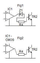
The purpose of the zener diode shown throughout these circuits (Fig 1) is to ensure that when the output of the operational amplifier drops below a few volts the transistor TR2 will be in its off state. It also allows the output of the op amp to be "around" half the op amp's supply voltage in normal operation.
A better way is to use a CMOS op amp; this has the advantage of allowing input and output voltages down to the negative (zero) rail. CMOS Op amps are less common, but still widely available, (CPC, Mouser etc) and TI LMC662, or TS 272 will work well.
In this case the zener diode can be omitted (Fig 2) as the output will reach 0V and turn off TR2. This also allows variable outputs to be controlled almost down to zero volts.
CMOS op amps are dsigned for single supply use at between 5V - 12V and the amplifier inputs also must not exceed the value of the supply voltage.
Heat Sinks
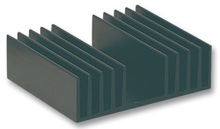 Power transistors need to be mounted on a suitable heat sink. First you must calculate the maximum expected power dissipation. Suppose your supply provides 20-30V at 2A and has an unregulated source at 38V. The Pmax = 38 - 20 = 18V * 2A = 36W. Suppose we choose a TIP120.
The transistor junction must be maintained at a temperature below about 120C (the transistor will be destroyed at 150C).
Suppose ambient temperature is 20C. The TIP120 has a thermal resistance (junction - case) of 2 deg C per watt.
Mounted on a heat sink as shown here (which has a thermal resistance of 1.4C per watt) gives
Rth total = 2.0 + 1.4 = 3.4C per watt
and 3.4C per watt * 36W = 122C. Add on 20C ambient = 142C and the transistor is COOKED!
Clearly we need to reduce the thermal resistance.
We could:
- use a TIP162. Rth total = 1.0 + 1.4 = 2.4C per watt * 36W = 86C + 20C = 106C -- which is fine.
- mount 2 * TIP120 on the same heat sink. Using two shares the power between them.
- Use a bigger (more expensive) heat sink.
- Use a fan to force-cool the heat sink.