John Errington's Data Conversion Website
Analog to Digital converters (ADC's)
There are many different techniques used for analog to digital conversion. They are summarized in the table below showing their particular strengths and weaknesses. Click on the technique for an explanation.
| Technique | Example | Resolution | Speed | Comment |
| Flash | MAX 100 | 8 bit | 250M | video: high power consumption: sparkle codes |
| Pipeline | MAX 1200 | 16 bit | 1M | fast; low power consumption; self calibrating |
| Algorithmic | MAX1298 | 12 bit | similar to S/A but gaining popularity easily implemented | |
| Successive approximation | MAX 195 | 16 bit | 85k | economical & widely used; needs steady signal |
| Sigma-Delta | MAX 1400 | 18 bit | 480 | recently introduced & gaining popularity |
| Integrating | MAX 132 | 18 bit | 100 | converts voltage to time, then measures time: excellent noise rejection, can be very precise |
| Voltage to frequency converter | LM331 | n/a | 100k | telemetry |
Direct-conversion (FLASH) ADCs
Of the five techniques mentioned, one of the fastest is direct conversion, better known as "flash" conversion. ADCs based on this architecture are extremely fast and perform their multibit conversion directly, but they require intensive analog design to manage the large number of comparators and reference voltages required. As shown in Figure 1, a converter with N-bit resolution has 2N-1 comparators connected in parallel, with reference voltages set by a resistor network and spaced VFS/2N (~1 least significant bit, or LSB) apart.
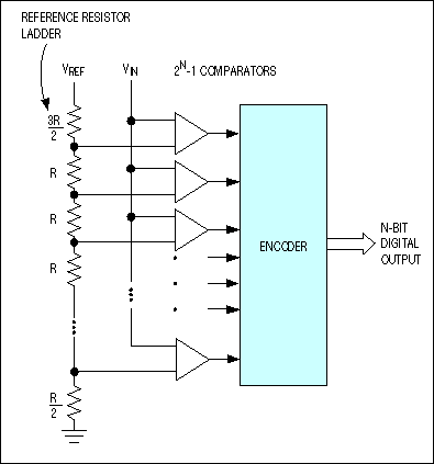
Figure 1. ADCs based on the direct-conversion architecture (better known as flash converters) include 2N-1 comparator banks and a reference resistor-divider network.
A change of input voltage usually causes a change of state in more than one comparator output. These output changes are combined in a decoder-logic unit that produces a parallel N-bit output from the converter. Although flash converters are the fastest types available (products like the future MAX104 offer sampling rates to 1GHz), their resolution is constrained by the available die size and by excessive input capacitance and power consumption caused by the large number of comparators used. Their repetitive structure demands precise matching between the parallel comparator sections, because any mismatch can cause static error such as a magnified input offset voltage (or current).
Flash ADCs are also prone to sporadic and erratic outputs known as "sparkle codes." Sparkle codes have two major sources: Metastability in the 2N-1 comparators, and thermometer-code bubbles.
Mismatched comparator delays can turn a logical 1 into 0 (or vice versa), causing the appearance of "bubbles" in an otherwise normal thermometer code. Because the ADC's encoder unit cannot detect this error, it generates an out-of-sequence code that also appears as an output "spark."
Another concern with flash ADCs is its die size, which is nearly seven times larger for an 8-bit flash converter than for the equivalent pipelined ADC. In further contrast to pipeline designs, the flash converter's input capacitance can be six times higher and its power dissipation twice as high.
Pipelined ADCs
The pipelined analog-to-digital converter (ADC) has become the most popular ADC architecture for sampling rates from a few megasamples per second (MS/s) up to 100MS/s+, with resolutions from 8 bits at the faster sample rates up to 16 bits at the lower rates. These kinds of resolutions and sampling rates cover a wide range of applications, including CCD imaging, ultrasonic medical imaging, digital receiver, base station, digital video (for example, HDTV), xDSL, cable modem, and fast Ethernet.
Lower-sampling-rate applications are still the domain of the successive approximation register (SAR) and integrating architectures (and more recently oversampling/sigma-delta ADCs), whereas the highest sampling rates (a few hundred MS/s or higher) are still obtained using flash ADCs and their variants. However, it is safe to say that pipelined ADCs of various forms have improved greatly in speed, resolution, dynamic performance, and low power in recent years.
Pipelined ADC Architecture
Figure 1 shows a possible block diagram of a 12-bit pipelined ADC.
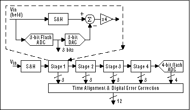 Figure 1. Pipelined ADC with four 3-bit stages (each stage resolves 2 bits)
Here, the analog input VIN is first sampled and held steady by a sample-and-hold (S&H), while the flash ADC in stage one quantizes it to 3 bits. The 3-bit output is then fed to a 3-bit DAC (accurate to about 12 bits), and the analog output is subtracted from the input. This "residue" is then gained up by a factor of 4 and fed to the next stage (stage two). This gained-up residue continues through the pipeline, providing 3 bits per stage until it reaches the 4-bit flash ADC, which resolves the last 4LSB bits. Because the bits from each stage are determined at different points in time, all the bits corresponding to the same sample are time-aligned with shift registers before being fed to the digital-error-correction logic. Note that as soon as a certain stage finishes processing a sample, determining the bits and passing the residue to the next stage, it can start processing the next sample due to the sample-and-hold embedded within each stage. This pipelining action accounts for the high throughput.
Latency
Because each sample has to propagate through the entire pipeline before all its associated bits are available for combining in the digital-error-correction logic, data latency is associated with pipelined ADCs. In the example in Figure 1, this latency is about three cycles (see Figure 2).
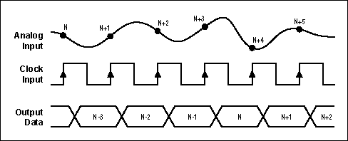
Figure 2. Data latency in a pipelined ADC
Digital Error Correction
Most modern pipelined ADCs employ a technique called "digital error correction" to greatly reduce the accuracy requirement of the flash ADCs (and thus the individual comparators). In Figure 1, notice that the 3-bit residue at the summation-node output has a dynamic range one-eighth that of the original stage-one input (VIN), yet the subsequent gain is only 4. Therefore, the input to stage two occupies only half the range of the 3-bit ADC in stage two (that is, when there is no error in the first 3-bit conversion in stage one).
If one of the comparators in the first 3-bit flash ADC has a significant offset, when an analog input close to the trip point of this comparator is applied, an incorrect 3-bit code and thus an incorrect 3-bit DAC output would result, producing a different residue. However, it can be proven that, as long as this gained-up residue doesn't over-range the subsequent 3-bit ADC, the LSB code generated by the remaining pipeline when added to the incorrect 3-bit MSB code will give the correct ADC output code. The implication is that none of the flash ADCs in Figure 1 has to be as accurate as the entire ADC. In fact, the 3-bit flash ADCs in stages one through four require only about 4 bits of accuracy.
The digital error correction will not correct for errors made in the final 4-bit flash conversion. However, any error made here is suppressed by the large (44) cumulative gain preceding the 4-bit flash, requiring the final stage to be only more than 4-bits accurate.
In the example in Figure 1, although each stage generates 3 raw bits, because the interstage gain is only 4, each stage (stages one to four) effectively resolves only 2 bits. The extra bit is simply to reduce the size of the residue by one half, allowing extra range in the next 3-bit ADC for digital error correction, as mentioned above. This is called "1-bit overlap" between adjacent stages. The effective number of bits of the entire ADC is therefore 2 + 2 + 2 + 2 + 4 = 12 bits.
Component Accuracy
Digital error correction does not correct gain or linearity errors in the individual DAC and gain amplifiers. In particular, the front-end S&Hs and DAC need about 12-bit accuracy, whereas the components in subsequent stages require less accuracy (for example, 10-bit for stage two, 8-bit for stage three, and so forth) because their error terms are divided down by the preceding interstage gain(s). This fact is often exploited to further save power by making the pipelined stages progressively smaller.
In most pipelined ADCs designed with CMOS or BiCMOS technology, the S&H, the DAC, the summation node, and the gain amplifier are usually implemented as a single switched-capacitor circuit block called a multiplying DAC (MDAC). The major factor limiting MDAC accuracy is the inherent capacitor mismatch. A purely bipolar implementation would be more complicated and would suffer mainly from resistor mismatch in the current source DAC and the interstage gain amplifier.
In general, for about 12 bits of accuracy or higher, some form of capacitor/resistor trimming or digital calibration is required, especially for the first couple of stages.
Digital Calibration
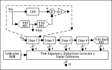 The MAX1200/MAX1201/MAX1205 family * (16-bit 1MS/s, 14-bit 1MS/s and 2MS/s ADC) employs digital calibration to ensure its excellent accuracy and dynamic performance. The MAX1200 family is a CMOS pipelined ADC with four 4-bit stages (with 1-bit overlap) and a 5-bit flash ADC at the end, giving a total of 3 + 3 + 3 + 3 + 5 = 17 raw bits (see Figure 3). The extra 1 to 3 bits are required by the digital calibration to quantize the error terms to greater accuracy than the ADC itself and are discarded to give either 14 bits or 16 bits overall.
Calibration starts from the MDAC in the third stage; beyond the third stage the MDAC error terms are small enough that calibration is not needed. The third-stage output is digitized by the remaining pipelined ADC, and the error terms are stored in on-chip RAM. Once the third MDAC is calibrated, it can be used to calibrate the second MDAC in a similar fashion. Likewise, once the second and third MDAC are calibrated, they are used to calibrate the first MDAC. Averaging is used (especially in the first and second MDAC) to ensure that the calibration is noise-free. During normal conversions, those error terms are recalled from the RAM and are used to adjust the outputs from the digital-error-correction logic.
Algorithmic ADC
An algorithmic (or cyclic) ADC performs the conversion in an iterative process in a similar way to a pipellined architecture
Successive-approximation ADCs
The conversion technique based on a successive-approximation register (SAR), also known as bit-weighing conversion, employs a comparator to weigh the applied input voltage against the output of an N-bit digital-to-analog converter (DAC). Using the DAC output as a reference, this process approaches the final result as a sum of N weighting steps, in which each step is a single-bit conversion.
The first step stores the DAC's most significant bit (MSB) in the SAR, and the next step compares that value (the MSB) against the input. The comparator output (high or low) is fed to the DAC as a correction before the next comparison is made (Figure 2). Clocked by a logic control circuit, the SAR continues this weighing and shifting process until it completes the LSB step, which produces a DAC output within ±1/2LSB of the input voltage. As each bit is determined, it is latched into the SAR as part of the ADC's output.
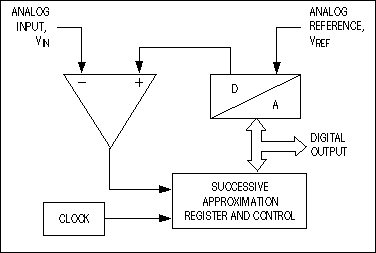
SAR converters consist of one comparator, one DAC, one SAR, and a logic control unit. They sample at rates to 1Msps, draw low supply current, and offer the lowest production cost, but their analog design is intensive and time consuming. Compared to a pipelined conversion structure, SAR ADCs provide a lower input bandwidth and sampling rates without latency problems.
Integrating ADCs
Integrating ADCs, also called dual- or multi-slope data converters, are among the most popular converter types. The classical dual-slope converter has two main sections: a circuit that acquires and digitizes the input, producing a time-domain interval or pulse sequence; and a counter that translates the result into a digital output value (Figure 3).
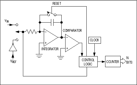
Figure 3. For slowly changing signals, one of the slowest but simplest conversion techniques employs an integrator that charges with the input voltage and discharges with an opposite-polarity reference voltage.
The dual-slope converter employs an analog integrator with switched inputs, a comparator, and a counter unit. The input voltage is integrated for a fixed time interval (TCHARGE) that usually corresponds to the maximum count of the internal counter unit (Figure 4). At the end of this interval the device resets its counter and applies an opposite-polarity (negative) reference to the integrator input. With this opposite-polarity signal applied, the integrator "deintegrates" until its output reaches zero, which stops the counter and resets the integrator.
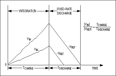
Charge gained by the integrator capacitor during the first, integrating/charging interval (TCHARGE/|VIN|) must equal that lost during the second, deintegrating/discharging interval (TDISCHARGE/|VREF|). Then the binary output is proportional to the ratio of these time intervals relative to the full count. TDISCHARGE at the end of the second interval corresponds to the ADC's output code. The relationship of VIN, VREF, TCHARGE, and TDISCHARGE is as follows:

For very high precision and accuracy a self-calibration cycle can be introduced. Converters using this technique are referred to as "quad slope" converters.
Sigma-delta (S-D) ADCs
Sigma-delta (S-D) converters have relatively simple structures. Also called oversampling converters, they consist of a S-D modulator followed by a digital decimation filter (Figure 5). The modulator, whose architecture is similar to that of a dual-slope ADC, includes an integrator and a comparator with a feedback loop that contains a 1-bit DAC. This internal DAC is simply a switch that connects the comparator input to a positive or negative reference voltage. The S-D ADC also includes a clock unit that provides proper timing for the modulator and digital filter.
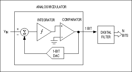
Figure 5. The two major building blocks of a sigma-delta converter are the analog modulator and the digital decimation filter.
Low-bandwidth signals applied to the input of a S-D ADC are quantized with very low (1-bit) resolution, but with a high sampling frequency of 2MHz or higher. Combined with digital post-filtering, this oversampling reduces the sampling rate to about 8kHz and increases the ADC's resolution (i.e., dynamic range) to 16 bits. Although slower than pipeline ADCs and limited to lower input bandwidths, the S-D principle has developed a strong position in the data-converter market. It offers three major advantages:
- Low-cost, high-performance conversion
- Digital filter included with the conversion circuitry
- DSP-compatible for system integration